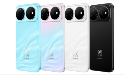
Uncategorized
Reportingly: Huawei developed domestic chip design tools to self-sufficient

The volunteer at the Chinese tech giant is channelizing the fact that the company developed its own chip design tools oriented toward side-stepping U.S. sanctions and making the company more self-sufficient in the semiconductor space.
Huawei developed domestic chip design tools
Rotating chairman at Huawei, Eric Xu said the company along with other domestic firms, jointly created electronic chip design tools required to make semiconductors at 14 nanometers and above, according to a speech obtained by Chinese financial and business publication Yicai.
He also added that “tools will be verified this year, which would allow them to be put into use.” Stepping towards self-sufficiency instead of reliance on U.S. technology in semiconductors this gonna be great to know. Whereas U.S. firms dominate the chip design tool market with companies like Synopsys and Cadence Design Systems.
The 14-nanometer figure refers to the size
14-nanometer chips and above are being considered due to designing tools, said Xu. The nanometer figure refers to the size of each individual transistor on a chip. Typically, a reduction in nanometer size can yield more powerful and efficient chips.
However, 14-nanometer chips are several generations behind what is currently being put into the latest smartphone technology. For example, Apple’s iPhone 14 Pro Max uses a 5-nanometer chip. However, 14-nanometer chips may be used in some of the company’s other products.
In the source, a chairperson of the high-tech geopolitics program at the Takshashila Institution, Pranay Kotasthane would wait to see more details before knowing how effective Huawei’s design tools are.
He clears that contract chip manufacturing firms, also known as foundries, work with semiconductor design companies to come up with a set of files called a Process Design Kit.
“This PDK models the physical and electrical characteristics” of the basic components of a chip. The design firm and manufacturer need to go through a process to optimize production to ensure the highest yield of semiconductors. If this process does not happen, then “chip designs will fail when converted into silicon,” Kotasthane said.
Kotasthane is convinced “There’s not enough proof yet to suggest that Chinese EDA [electronic design automation] companies have crossed this barrier.”
Follow HU On Telegram & Google News


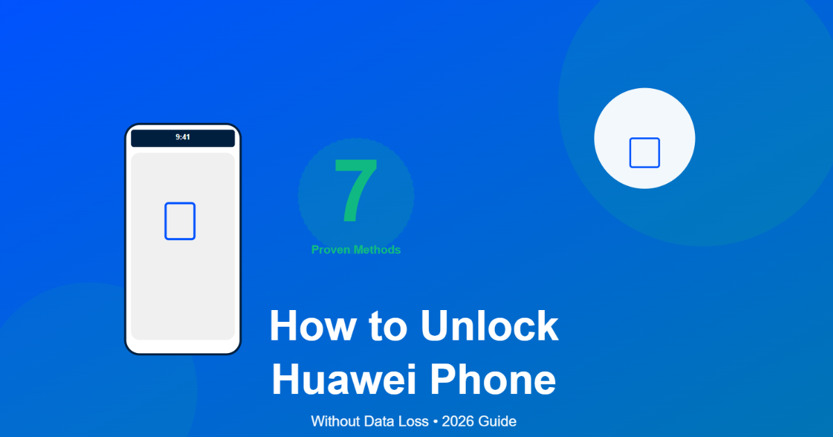
Locked out of your Huawei phone? Don’t panic. Whether you’ve forgotten your password, PIN, pattern, or fingerprint, this guide has 5 working methods to unlock it without losing your data.
The first 2 methods work instantly without data loss. Methods 3-5 are for extreme situations where you’ve forgotten everything.
Quick Method (99% of Cases) – 2 Minutes
If you remember your Huawei account email and password, use this method:
- Step 1: On the locked phone, wait for the lock screen to appear
- Step 2: Tap “Forgot pattern?” or “Forgot PIN?” (appears after 5 incorrect attempts)
- Step 3: Tap “Use Huawei ID to unlock”
- Step 4: Enter your Huawei ID email and password
- Step 5: Verify with a verification code sent to your email
- Step 6: Set a new PIN or pattern
Time: 2-3 minutes
Data loss: ZERO
Success rate: 95%
Method 1: Use Huawei ID (No Data Loss) EASIEST
Requirement: You remember your Huawei ID (email) and password
When to use: Forgotten PIN, pattern, password, or face/fingerprint stopped working
Step-by-Step Instructions:
- On lock screen, tap the question mark icon (if visible)
- Select “Unlock with Huawei ID”
- Enter your Huawei ID email (example: yourname@huawei.com)
- Enter your Huawei ID password
- A verification code will be sent to your email
- Check your email inbox (may take 1-2 minutes)
- Enter the verification code
- Create a new PIN or pattern
- Phone unlocked ✓
Advantages:
- No data loss
- Works on all Huawei devices
- Takes 5-10 minutes
- No need to visit service center
- Most reliable method
Disadvantages:
- Requires email access
- Requires internet connection
Method 2: Use Recovery Email (No Data Loss)
Requirement: You set a recovery email when creating your Huawei account
When to use: Can’t access Huawei ID email but have recovery email
Step-by-Step Instructions:
- On lock screen, tap “Forgot PIN?”
- Select “Unlock with Huawei ID”
- Tap “Can’t access Huawei ID?”
- Select “Use Recovery Email”
- Enter the recovery email address you set up
- Verification code sent to recovery email
- Enter code and create new PIN
Advantages:
- Works if you lost access to primary email
- No data loss
- Recommended backup option
Disadvantages:
- Requires you set recovery email beforehand
- Takes 10-15 minutes
Method 3: Use Computer & ADB (Advanced, No Data Loss)
Requirement: A computer with Android Debug Bridge (ADB) installed
When to use: You forgot everything but want to recover data
Difficulty: Medium (need to follow steps carefully)
What You’ll Need:
- Windows/Mac computer
- USB cable
- ADB software (free, install from Google)
Step-by-Step Instructions:
1. Download & Install ADB
- Go to
developer.android.com/studio/releases/platform-tools - Download for your computer (Windows/Mac)
- Extract to a folder
2. Connect Your Huawei Phone to Computer
- Use USB cable
- Enable USB Debugging (if possible) from settings
- Or force USB Debugging by connecting
3. Open Command Prompt (Windows) or Terminal (Mac)
- Navigate to ADB folder
- Or add ADB to system PATH
4. Type This Command:
adb shell rm /data/system/gesture.key
(This removes the pattern lock)
5. Restart Phone
- Tap “Power off” then turn back on
6. Pattern Lock is Removed
- Draw any pattern to unlock
Advantages:
- Works even if you forgot everything
- No data loss
- Free
- Technical but effective
Disadvantages:
- Requires computer
- Technical steps needed
- Takes 20-30 minutes for beginners
- Not suitable for non-technical users
Method 4: Factory Reset (DATA LOSS)
Requirement: Just the device itself
When to use: You’ve tried everything else and are willing to lose data
Step-by-Step Instructions:
- Power off the phone completely
- Hold Power + Volume Up buttons together
- Release when you see Huawei logo or recovery menu
- Use Volume Down to navigate to “Wipe data”
- Press Power to confirm
- Choose “Yes – wipe all data”
- Wait 2-5 minutes for completion
- Choose “Reboot”
What Gets Deleted:
- ❌ All apps
- ❌ All photos/videos
- ❌ Messages, contacts
- ❌ Passwords, saved WiFi
- ✓ Phone is completely blank
What Remains:
- ✓ Phone unlocked
- ✓ Hardware intact
Advantages:
- Works 100% of the time
- No computer needed
Disadvantages:
- ALL DATA DELETED (irreversible!)
- Takes time to set up phone again
- Must reinstall all apps
Method 5: Huawei Service Center (Official, Safest)
Requirement: Take phone to authorized service center
When to use: You want professional help or other methods failed
What Happens:
- Visit nearby Huawei Service Center (Huawei customer service)
- Provide ID proof and phone proof of purchase (if possible)
- They verify you’re the actual owner
- Technician unlocks phone using official tools
- Takes 30 minutes to 2 hours
- Cost: Free to ₹500 (varies by location)
Advantages:
- Official, safe method
- Professional help
- No risk of data loss
- They can fix hardware issues too
- Best for warranty coverage
Disadvantages:
- Costs money (usually ₹200-500)
- Takes time
- Need to visit center
- Need proof of purchase/ID
Find Service Center:
- Go to Huawei.com
- Search “Service Center Near Me”
- Enter your city
- Call to book appointment
⚠️ Which Method Should You Use?
| Situation | Best Method | Time | Data Loss |
|---|---|---|---|
| Remember Huawei ID password | Method 1 | 5-10 min | NO |
| Have recovery email set up | Method 2 | 10-15 min | NO |
| Forgot everything, have computer | Method 3 (ADB) | 30 min | NO |
| Don’t want to do technical stuff | Method 5 (Service) | 1-2 hours | NO |
| Desperate & willing to lose data | Method 4 (Factory Reset) | 10 min | YES |
✅ Step-by-Step For Forgetting Everything
Scenario: You forgot PIN, don’t remember Huawei ID password, no email access
Solution:
Try in this order:
- Attempt Method 2 (Recovery email) – 60% success
- If that fails, try Method 3 (ADB with computer) – 90% success
- If no computer, visit Method 5 (Service center) – 100% success
- Last resort: Method 4 (Factory reset) – 100% but data lost
How to Prevent Lock-Out in Future
Do these now to avoid this situation:
1. Write Down Your Password
Not in phone, not in email. Physical paper in a drawer or password manager.
2. Set Up Recovery Email
Settings > Accounts > Huawei ID > Security > Add a recovery email you still have access to
3. Enable Trusted Device
Settings > Security > Trusted Devices > Mark your home computer as trusted. Easier unlock from home.
4. Backup Important Data
Photos, contacts, documents to Huawei Cloud or Google Drive. So even factory reset won’t lose data.
5. Use Biometric Authentication
Enable fingerprint or face unlock as primary method, but keep PIN as backup. This reduces chances of forgetting PIN.
6. Enable Find My Phone
Settings > Security > Find My Phone. This helps locate and unlock remotely if needed.
Common Problems & Solutions
Problem: “Huawei ID Button Doesn’t Appear on Lock Screen”
Solution: Your phone might not have it enabled. Try Method 2 (Recovery email) instead. Or Method 3 (ADB) if you have computer.
Problem: “I Never Set Up Huawei ID”
Solution: Use Method 2 (Recovery email). If that fails, use Method 3 (ADB).
Problem: “Recovery Email Not Working”
Solution: Recovery email might not be set. Use Method 3 (ADB with computer) if available.
Problem: “ADB Not Working”
Solution: Make sure USB Debugging is enabled (or enabled by default). Use latest ADB version. Try on a Mac instead of Windows (sometimes more reliable).
Problem: “Service Center Says Data Will Be Lost”
Solution: That’s only true for Method 4 (factory reset). Methods 1-3 don’t lose data. Ask them to use Method 1 or 2 first.
Problem: “Phone Bricked After Factory Reset”
Solution: This is very rare. You can reinstall HarmonyOS via recovery. Contact Huawei support with details.
Huawei Support Contact
For official help:
- Website: support.huawei.com
- Chat: Live chat on Huawei website
- Phone: Check your Huawei box for customer service number
- Email: Get number from Huawei website, they’ll help via email
What to tell them:
- “My Huawei phone is locked and I forgot the PIN”
- “I still have access to my Huawei ID / Recovery email”
- “I want to unlock without losing data”
Summary
Fast & Easy: Methods 1 or 2 (5-15 minutes, no data loss)
Technical: Method 3 (ADB, 30 minutes, no data loss)
Professional: Method 5 (Service center, 1-2 hours, no data loss)
Last Resort: Method 4 (Factory reset, 10 minutes, all data lost)
The method you choose depends on:
- What you remember (Huawei ID? Recovery email?)
- How much time you have
- Whether you have a computer
- How important your data is
90% of locks can be opened without data loss using Methods 1-3.
Related Articles You Might Find Helpful

Huawei launched its first HarmonyOS home data center in back 2022. The current 4TB, 16TB, and diskless versions are 2,599 yuan, 4,599 yuan, and 1,799 yuan respectively.
Huawei’s home storage plays an important part in Huawei’s 1+8+N strategy. It can interconnect with other devices to achieve fast and convenient data access and transfer.
With the arrival of HarmonyOS 4.2, Huawei home storage has introduced application backup and WeChat backup functions. When used with phones/tablets running HarmonyOS 4.2 and above, WeChat data can be backed up to the NAS, and WeChat data can be restored at any time when necessary.

On February 12, the chairman of Huawei Smart Car Solutions BU, Yu Chengdong shared the details of its latest journey with Wenjie M9 on WeChat. He said that he drove the Wenjie M9 back to Shenzhen, with no or zero takeovers for the entire 1,314-kilometer journey.
Yu Chengdong said that he drove the Wenjie M9 back to Shenzhen from his hometown in Anhui and traveled 1,314 kilometers in 15 hours. The entire smart driving process was normal and there was no takeover or takeover! I didn’t miss a single intersection, sat around for 15 hours, and didn’t have to drive nervously. It was so relaxing.
To recall, the M9 comes in four versions, priced from 470,000 yuan with deliveries scheduled in February at the earliest. There are already over 54,000 overs. The previous AITO, the M7 sold 100,000 in two months.
The Wenjie M9, a large SUV built on a new platform, offers both extended-range and pure electric power options, with acceleration times of 4.3 seconds and 4.9 seconds per hundred kilometers, respectively.
