


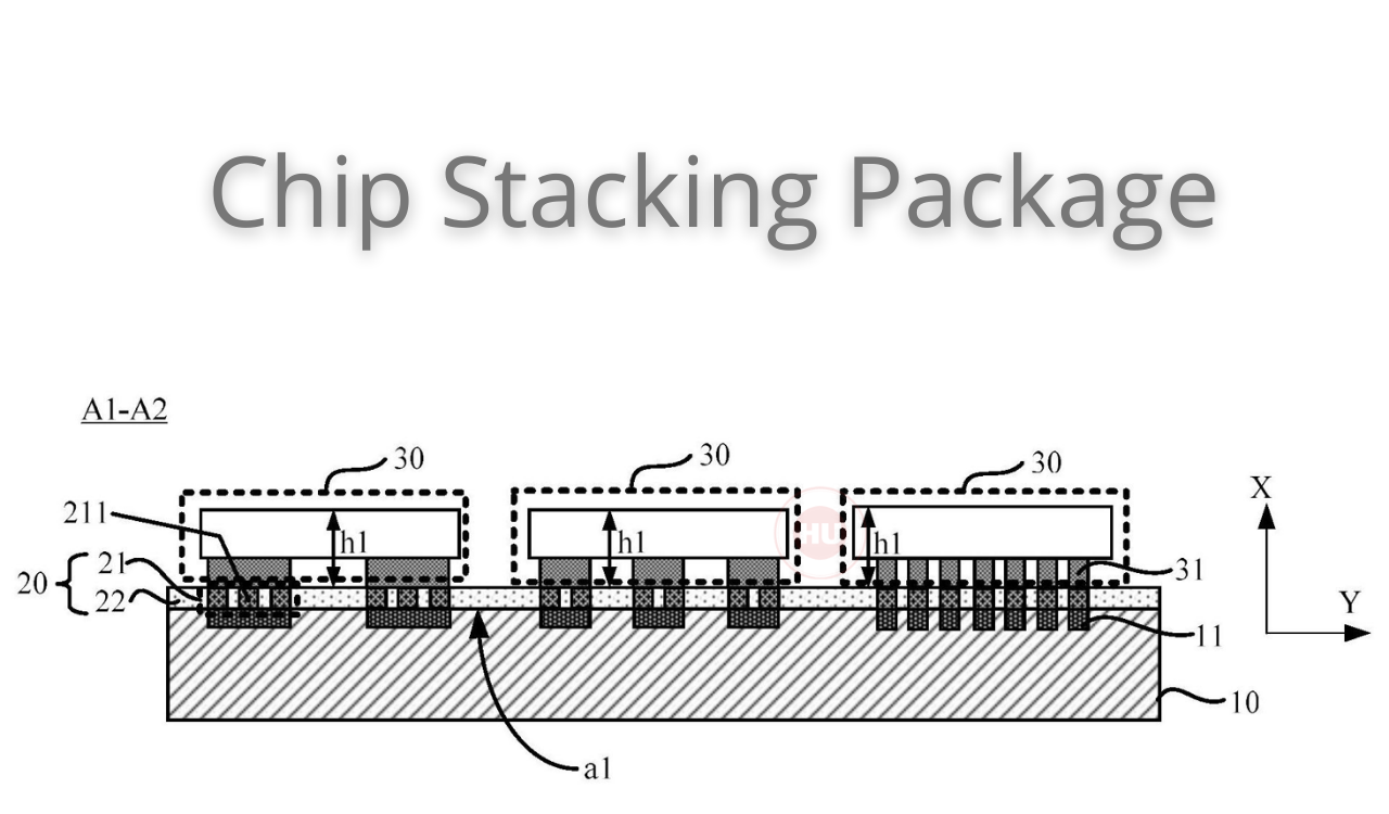
According to the State Intellectual Property Office, Huawei published a patent for “chip stacking packaging structure, packaging method, and electronic equipment”, with the publication number CN114450786A.
As per the patent details, the application relates to the field of electronic technology and is used to solve the problem of how to reliably bond multiple secondary chip stacking units to the same main chip stacking unit.
The patent documents show that the chip-on-package structure includes:
- A main chip stacking unit has a plurality of main pins on the first surface that are insulated and arranged at intervals.
- The first bonding layer is arranged on the first surface; the first bonding layer includes a plurality of bonding components that are insulated and arranged at intervals.
- Each of the plurality of bonding assemblies includes at least one bonding portion, any two bonding portions are insulated and disposed of, and any two bonding portions have the same cross-sectional area; the plurality of bonding assemblies are respectively connected to the plurality of main pin keys combine.
- A plurality of secondary chip stacking units is arranged on the surface of the first bonding layer on the side away from the main chip stacking unit.
The sub-chip stacking unit has a plurality of micro-bumps that are insulated and spaced apart; each of the plurality of micro-bumps is bonded to one of the plurality of bonding components.


Source:
IThome