Huawei News
Huawei published a patent for a chip stacking package and terminal equipment

Huawei has officially disclosed a patent for a chip stacking package and terminal equipment to solve the problem of high cost caused by the use of through-silicon via technology.
Huawei published a chip-related patent on April 5, with the publication number CN114287057A. The patent details show that this is a chip stacking package and terminal equipment, involving the field of semiconductor technology, which can solve the problem of high cost caused by the use of through-silicon via technology while ensuring the power supply demand.
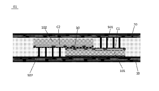
The patent documents show that the chip stack package (01) includes:
A first chip (101) and a second chip (102) disposed between the first wiring structure (10) and the second wiring structure (20);
The active surface (S1) of the first chip (101) faces the active surface (S2) of the second chip (102);
The active surface (S1) of the first chip (101) includes a first overlapping area (A1) and a first non-overlapping area (C1), and the active surface (S2) of the second chip (102) includes a second overlapping area (C1) an overlapping area (A2) and a second non-overlapping area (C2);
The first overlapping area (A1) overlaps the second overlapping area (A2), and the first overlapping area (A1) and the second overlapping area (A2) are connected;
The first non-overlapping region (C1) is connected with the second wiring structure (20);
The second non-overlapping region (C2) is connected with the first wiring structure (10).


We often get caught up in the numbers game when talking about new smartphones. We look at clock speeds, gigabytes, and chip sizes. But if you think about it, what makes you actually love using your phone every day? It is usually the little things—the way it vibrates when you type, the fullness of the sound when you watch a video, and how fast the cloud services behind your apps respond.
Huawei is tackling both sides of this coin. Brand new leaks and event announcements show that the company is working on a dual strategy. On one hand, the upcoming Mate 90 series is focusing heavily on the physical, everyday features we often overlook. On the other hand, the corporate side just laid out a massive plan for autonomous AI and cloud security at their INSPIRE 2026 event in Shanghai. Let’s break down what all of this means for you.
The Mate 90 Look: Focusing on the Features We Actually Touch
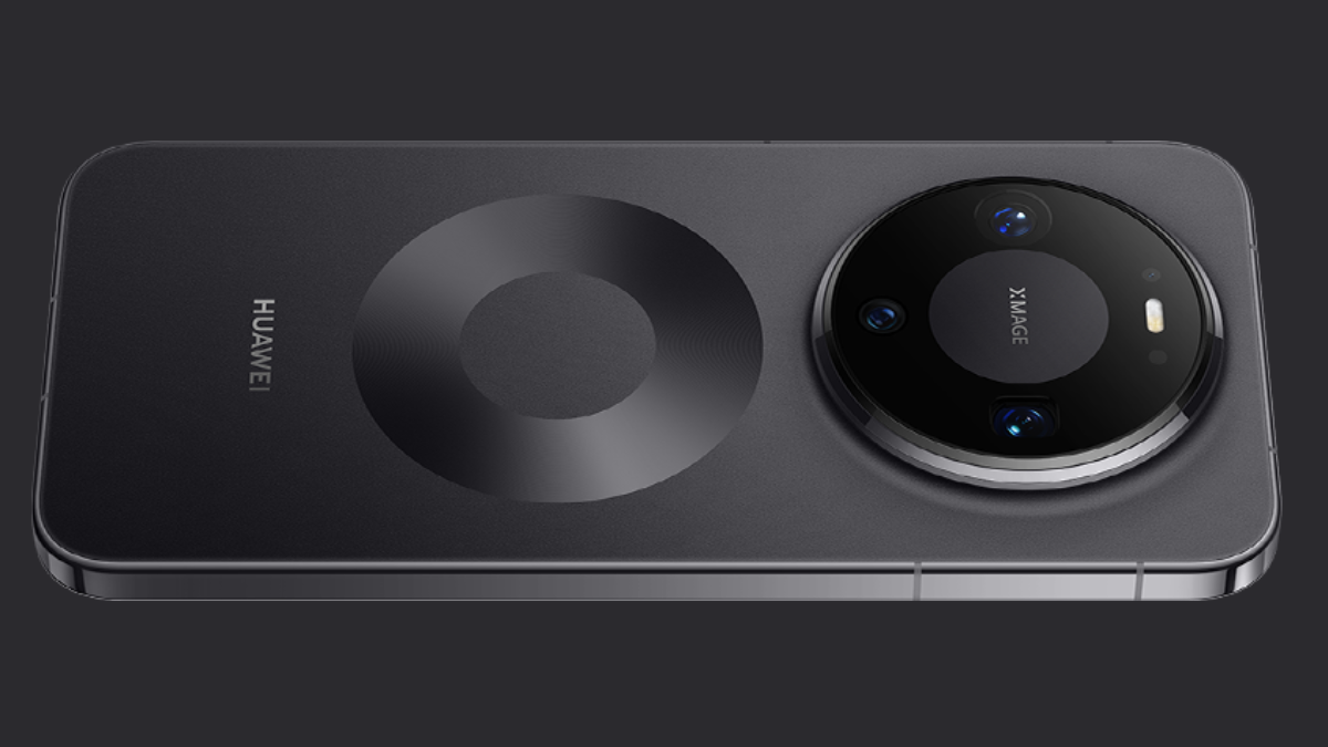
The upcoming Huawei Mate 90 series is already generating a ton of buzz because it is shifting its launch window to September. It is also bringing a brand new Kirin chip built with an advanced vertical layout to challenge global 3nm standards. But the latest supply chain whispers tell us that Huawei is spending just as much energy on the parts of the phone you physically interact with every single second.
Better Haptics: The New X-Axis Motor
Have you ever typed on a phone that felt hollow or mushy? It completely ruins the experience. Huawei wants to fix that by adding a brand-new, ultra-responsive X-axis linear haptic motor to the Mate 90 lineup. Instead of a generic buzz, this motor can produce crisp, tiny vibrations that mimic real physical buttons. Whether you are typing a quick text, scrolling through a menu, or playing a mobile game, the phone will give you clean, realistic feedback that makes the software feel alive.
Upgraded Sound: Immersive Stereo Speakers
Another big upgrade is coming to the audio setup. Most of us watch videos, take video calls, or stream music directly from our phone speakers without plugging in headphones. The Mate 90 series is rumored to feature a redesigned stereo speaker chamber system. By reworking the physical space inside the phone, Huawei is aiming for much deeper bass and clear, separated audio. It means you won’t have to cup your hand around the bottom of your phone just to hear a podcast while cooking dinner.
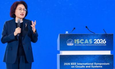
Huawei Cloud INSPIRE 2026: Moving Into Agentic Infrastructure
While the consumer team is polishing the physical hardware, the enterprise division is entirely focused on the future of artificial intelligence. Live from the West Bund International Convention Center in Shanghai, the Huawei Cloud INSPIRE 2026 summit just wrapped up. The big takeaway? Cloud computing is shifting from basic storage to what they call “Agentic Infrastructure.”
What is Agentic Infrastructure?
Think of normal AI as a tool that only answers when you ask it a direct question. An AI Agent, however, is different. It can think ahead, plan multi-step tasks, and make independent choices to help run a business or manage data.
Huawei’s new Agentic Infrastructure is a cloud setup built from the ground up to support thousands of these autonomous digital workers. It combines massive processing power with smart software, ensuring these AI systems can run continuously without lagging or crashing the servers.
Five Big Upgrades for AI Security and Keeping Things Legal
As AI grows more independent, security becomes a massive headache. If an AI agent is making decisions for a business, how do you keep its data safe? And how do you make sure it follows local privacy laws?
To answer this, Huawei Cloud announced five major security upgrades to its global portfolio. These upgrades act like a digital security guard, protecting sensitive data, keeping a strict eye on how AI models behave, and making sure everything complies with the changing regulatory rules in over 70 countries. It is all about turning AI from a wild, experimental tool into a safe, reliable coworker.
Connecting Your Phone to the Cloud
Why should the average user care about corporate cloud summits in Shanghai? Because the two worlds are rapidly merging. The advanced haptics, better speakers, and next-gen Kirin chips on the Mate 90 are just the gatekeepers. The real magic happens when those devices connect to a highly secure, intelligent cloud network.
When your phone can talk to a secure cloud infrastructure instantly, your voice assistants become smarter, your photo organization happens in a flash, and your data stays completely locked down away from prying eyes.
Conclusion: A Smarter, More Complete Tech Setup
Huawei is proving that a true flagship experience requires looking at the whole picture. By upgrading the overlooked physical hardware on the Mate 90 and building a secure foundation for autonomous AI in the cloud, they are preparing for the next big era of tech. Keep your eyes on September—it is going to be a very interesting fall season for tech fans!
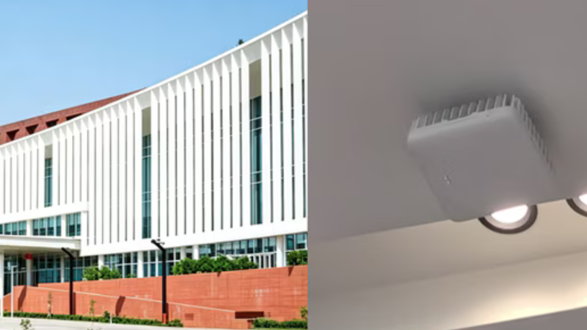
Two tech companies, MTN Zambia and Huawei, have teamed up to fix a big problem: slow internet inside busy buildings. They just installed a brand-new system at the Mulungushi International Conference Center in Zambia, and it is the first time this specific technology has been used anywhere in the world.
Why was this needed?
More and more people in Zambia are using mobile internet to watch high-definition videos, live stream, and use cloud services. This makes the internet very slow in crowded places like airports, shopping areas, and big conference centers.
Before this new upgrade, the internet inside the Mulungushi Center was struggling. The outside cell towers couldn’t send strong signals through the walls, and the old indoor antennas couldn’t handle fast 5G speeds.
What is the new solution?
Huawei created a small device called LampSite. Instead of installing five different boxes for different network speeds, they put everything into one single box.
Here is what this new system does:
- Super Fast Speeds: It combines different network bands (including 2G, 3G, 4G, and 5G) to give users download speeds up to 1 Gbps. This means videos and live streams won’t freeze or lag anymore.
- Easier and Cheaper to Set Up: Because it is a “5-in-1” box, the phone company needs half as many devices to cover the same area. This saves money and takes less time to install.
- Saves Energy: The device is smart. When nobody is using it, it goes to sleep to save power, making it eco-friendly.
Ready for the Future: It is built to handle even newer technologies coming down the road, like virtual reality (VR) and 3D glasses.
What the bosses are saying
Thomas Ngoma from MTN Zambia explained that this upgrade will give people the same fast internet inside the building as they get outside. It will make online video calls and apps run smoothly.
Dr. Philip Song from Huawei said they are proud of this new energy-saving system. They plan to install it in more crowded places like airports and business districts to help grow Zambia’s digital economy.
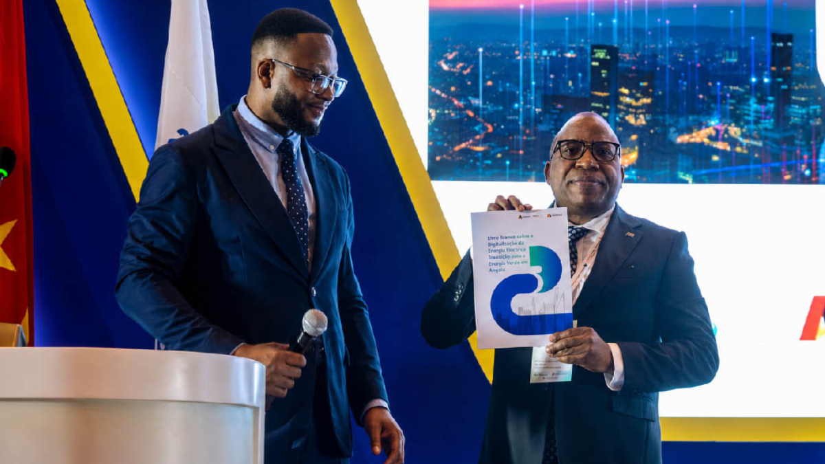
Imagine a future where a national power grid acts more like an organic, self-healing computer network than a chaotic mess of aging copper and transformers. If you think that sounds like science fiction, think again. On May 29, 2026, during the prestigious 2nd International Conference on Energy and Water in Luanda, Huawei teamed up with Angola’s Ministry of Energy and Water (MINEA) to release a historic white paper that promises to reshape the region’s entire power architecture.
The publication, aptly titled White Paper on Digitalization and Green Energy Transition of Angola’s Electric Power Industry, sets down an aggressive roadmap. It is a bold statement that digital modernization and structural economic survival are now inextricably linked.
A Visionary Leap for Angola’s Energy Grid
Angola is blessed with a staggering abundance of clean energy resources, positioning it beautifully to spearhead regional green integration across Southern Africa. But having raw potential means very little if your infrastructure is leaking energy like a sieve.
Dropping Watts, Adding Bits: The New Philosophy
To bridge this gap, the white paper relies heavily on a brilliant guiding principle: “more bits, less watts”. The idea is wonderfully simple yet revolutionary—by injecting massive digital intelligence (“bits”) into the grid, you can systematically optimize distribution and minimize pure power waste (“watts”). It’s about working smarter, not just pumping out more raw currents.
Resolving the Pains of Traditional Operational Models
Let’s be honest: traditional utility operations are feeling the strain. Arlindo Carlos, Angola’s Secretary of State for Energy and Water, frankly addressed the audience at the launch, pointing out the major bottlenecks plaguing legacy systems: heavy line losses, fragmented network management, and an expensive reliance on imported fuel. The status quo is no longer sustainable. By turning toward deep digital transformation, Angola intends to build a future power grid that is profoundly greener, smarter, and incredibly reliable.
Inside the Transformation: Merging Tech and Currents
So, how exactly does a world leader in telecommunications help stabilize a country’s power network? It happens by fundamentally shifting from hard iron to intelligent software.
The Power of Four Core Technology Clusters
The backbone of this collaboration involves fusing four vital technology domains into a unified ecosystem:
- Digital Technologies (Bits): Cloud analytics, automated software controls, and IoT tracking.
- Power Electronics (Watts): Next-gen converters and optimized hardware pathways.
- Thermal Management (Heat): Advanced cooling methodologies to minimize energy bleed.
- Energy Storage Management (Battery): Sophisticated, smart storage solutions to save power for when it’s needed most.
Evolving the Power Matrix: What Lies Ahead?
This initiative is not just a collection of theoretical ideas printed on glossy paper; it provides an explicit operational template for the upcoming years.
Intelligent Distribution and Advanced All-Optical Networks
Moving forward, the extensive, old-school infrastructure of the past will make way for automated, grid-forming energy storage systems and intelligent distribution grids. Backed by robust, high-speed all-optical communication networks, the grid can seamlessly detect faults, dynamically adjust power routing, and absorb fluctuating renewable energies from solar and hydro plants without breaking a sweat.
Conclusion: Lighting a Greener Path for Southern Africa
Ultimately, the joint white paper proves that the future of power isn’t merely about burning cleaner fuels—it is about managing existing resources with hyper-intelligence. Through the “more bits, less watts” doctrine, Huawei and MINEA are providing a shining template for the entire African continent. The digital power revolution has officially arrived, and it’s starting from the ground up!